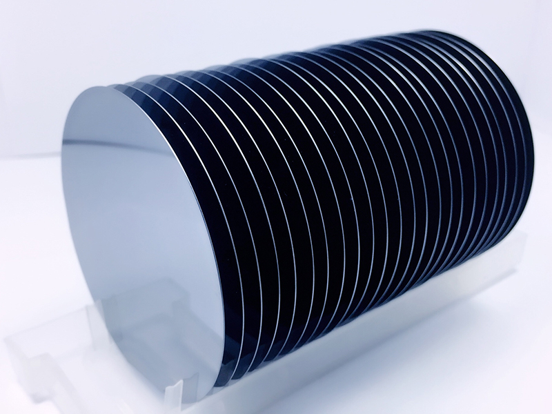
Si (Silicon) Optical-Grade Single Crystal
Description
Optical-grade silicon transmits 1.2–7 µm with peak 3–5 µm performance, the primary choice for MWIR thermal imaging and FTIR optics.
Request Information
Technical details
Advantages
- Good transmittance from 1.2 to 7.0 μm, with optimal performance in the 3–5 μm mid-wave infrared (MWIR) atmospheric window . Float Zone (FZ) material extends useful transmission to 8–15 μm with reduced absorption at 9 μm.
- High thermal conductivity: 273.3 W/(m·K), enabling efficient heat dissipation in high-power laser and thermal imaging systems.
- Lightweight and cost-effective: Lower density (2.33 g/cm³) than germanium (5.33 g/cm³) and zinc selenide (5.27 g/cm³), offering weight savings for the same aperture at lower material cost.
- High hardness and durability: Knoop hardness of 1150, providing excellent scratch resistance and long service life.
- Opaque in the visible: Completely blocks visible light (transparent only in IR), effectively suppressing stray light interference in infrared systems .
- Mature fabrication technology: Well-established Czochralski (CZ) and Float Zone (FZ) growth methods enable large-diameter windows and lenses at competitive prices .
Typical Specifications
- Chemical formula: Si
- Crystal structure: Face-centered cubic (diamond structure), space group Fd3m
- Transmission range: 1.2–7.0 μm (standard); 1.2–15 μm (FZ, extended)
- Refractive index: 3.41776 @ 10 μm; 3.4223 @ 5 μm; 3.4284 @ 3.5 μm
- Reflection loss: 46.1% @ 10 μm (both surfaces, uncoated)
- Absorption coefficient: 0.01 cm⁻¹ @ 3 μm; 0.03 cm⁻¹ @ 2.6–2.9 μm
- Melting point: 1420°C (1687 K)
- Density: 2.33 g/cm³
- Thermal expansion coefficient: 2.6 × 10⁻⁶/K
- Thermal conductivity: 273.3 W/(m·K)
- Knoop hardness: 1150
- Young’s modulus: 131 GPa
- Poisson‘s ratio: 0.266
- Purity: >99.999% (optical grade); 6N+ for FZ material
- Resistivity: >10 Ω·cm (n-type) or >30 Ω·cm (p-type) for standard optical grade; >100 Ω·cm for FZ
- Orientation: <100> or <111>
Main Applications
- Infrared windows and lenses: Primary application in thermal imaging cameras, FTIR spectrometers, infrared temperature measurement systems, and night-vision devices.
- MWIR optical systems: Lenses and windows for 3–5 μm atmospheric window applications, benefiting from high thermal conductivity and lightweight design.
- Laser mirror substrates: Used as substrates for CO₂ laser mirrors and other infrared laser optics.
- Infrared filters and beam splitters: Substrate material for infrared optical filters and polarizing components.
- Neutron targets: Bulk polished silicon used as neutron targets in physics experiments.
- Terahertz applications: High-resistivity FZ silicon is suitable for THz optical components due to low free-carrier absorption.